


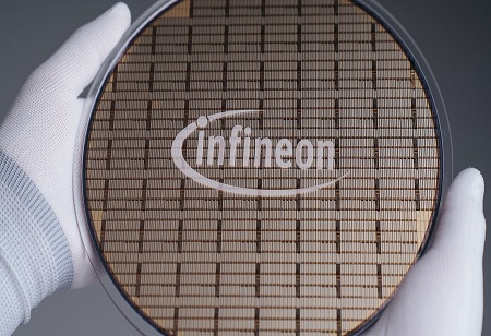
 Infineon Technologies AG has achieved a significant milestone by developing the world's first 300mm power gallium nitride (GaN) wafer technology. As the pioneer in mastering this cutting-edge technology within an established and scalable high-volume manufacturing environment, Infineon is set to greatly impact the GaN-based power semiconductor market. Producing chips on 300mm wafers is technologically superior and much more efficient than using 200mm wafers, as the larger wafer size yields 2.3 times more chips per wafer.
GaN-based power semiconductors find fast adoption in industrial, automotive, and consumer, computing, and communication applications, including power supplies for AI systems, solar inverters, chargers and adapters, and motor-control systems. State-of-the-art GaN manufacturing processes lead to improved device performance resulting in benefits in end customers’ applications as it enables efficiency performance, smaller size, lighter weight, and lower overall cost. Furthermore, 300mm manufacturing ensures superior customer supply stability through scalability.
“This remarkable success is the result of our innovative strength and the dedicated work of our global team to demonstrate our position as the innovation leader in GaN and power systems. The technological breakthrough will be an industry game-changer and enable us to unlock the full potential of gallium nitride. Nearly one year after the acquisition of GaN Systems, we are demonstrating again that we are determined to be a leader in the fast-growing GaN market. As a leader in power systems, Infineon is mastering all three relevant materials: silicon, silicon carbide and gallium nitride,” said Jochen Hanebeck, CEO of Infineon.
Infineon has successfully produced 300mm GaN wafers using an integrated pilot line within its existing 300mm silicon production facility in Villach, Austria. Building on its extensive experience in 300mm silicon and 200mm GaN production, Infineon plans to expand its GaN capacity in response to market demand. The advancement to 300mm GaN manufacturing will enable Infineon to play a significant role in the expanding GaN market, which is projected to reach several billion US dollars by the end of the decade.
This groundbreaking technological achievement underscores Infineon's role as a global leader in power systems and IoT semiconductors. By adopting 300mm GaN technology, Infineon aims to enhance current solutions and explore new application areas, offering a more cost-effective value proposition and addressing a broad spectrum of customer needs. The company will showcase its first 300mm GaN wafers at the Electronica trade show in Munich in November 2024.
A major benefit of 300mm GaN technology is its ability to leverage existing 300mm silicon manufacturing equipment, given the similarities in their production processes. Infineon’s established high-volume silicon 300mm production lines are well-suited for testing and implementing reliable GaN technology, facilitating a faster rollout and more efficient capital use. Scaling up 300mm GaN production will help achieve cost parity with silicon in terms of R DS(on) levels, leading to similar costs for comparable Si and GaN products.